Question 1Marks
a. Using shift instructions, write the codes for 8086 microprocessor.08
- Put the value
1234HinAXand multiply the value by 8.MOV AX, 1234H MOV CL, 3 SHL AX, CL - Divide the number
2345Hby 8 and put the quotient inAX.MOV AX, 2345H MOV CL, 3 SHR AX, CL
b. Write an assembly program to find the smallest number in the given array, 10
.MODEL SMALL
.STACK 100H

.DATA
    ARRAY DB 23, 21, 10, 12, 14
    LENGTH DW 5
    SMALLEST DB ?

.CODE
MAIN PROC
    MOV AX, @DATA
    MOV DS, AX

    LEA SI, ARRAY
    MOV CX, LENGTH
    MOV AL, [SI]
    MOV SMALLEST, AL
    INC SI
    DEC CX

FIND_MIN:
    CMP CX, 0
    JE DONE
    MOV AL, [SI]
    CMP AL, SMALLEST
    JGE SKIP
    MOV SMALLEST, AL

SKIP:
    INC SI
    DEC CX
    JMP FIND_MIN

DONE:
    MOV AH, 4CH
    INT 21H

MAIN ENDP
END MAIN
c. Give a logic instruction to do each of the following:02
- Set the MSB and LSB of
BLregister, leaving other bits unchanged.OR BL, 10000001b ; OR 1 -> Set - Clear the even numbered bits of register
AX, leaving the other bits unchanged.AND AX, 1010101010101010b ; AND 0 -> Clear
Question 2
a. Write a 8086 assembly code to solve the summation of the given series: 08
MOV SI, 1                ; Counter for Series
MOV BX, 0
MOV CX, 10               ; Defualt counter for LOOP

Continue:
	MOV AX, SI
	MUL SI               ; AX = AX * SI
	ADD BX, AX           ; ADD BX with AX
	INC SI
	LOOP Continue        ; Continue LOOP untill CX=0

MOV AX, BX               ; Store the sum of Series in AX
HLT
b. Name the registers that are involved in the stack operation of 8086 microprocessor. Suppose, the initial value of SP is 0100:1120 and FR=05H. Complete the table below for each instructions of the assembly language.10
| Instructions | SP | Value | AX | BX |
|---|---|---|---|---|
MOV AX, 1234H | - | - | ||
MOV BX, 2345H | - | |||
PUSH AX | ||||
POP BX | - | |||
PUSHF | ||||
POP BX | - | |||
NOT BX | - |
Tip
- When a word (16 bits) is pushed, the SP is decremented by 2. Conversely, when a word is popped, the SP is incremented by 2.
PUSHFpushes the 16-bit FLAGS register onto the stack (decrementing the Stack Pointer by 2), andPOPFpops a word from the stack into the FLAGS register
c. When the stack is completely filled the stack area, SP=0, if a data is pushed onto the stack, what would happen to SP?02
Ans: When the stack is completely filled and SP=0, if a data is pushed onto the stack, SP would wrap around to FFFFH. This is a stack overflow condition and causes serious problems. The data overwrites memory outside the intended stack area. It can corrupt code, data, or other critical memory regions.
Question 3
Question 4
a. Suppose, R1 contains 64H, CY=1. What will be the value of R1 and CY after each successive instruction is executed:10
RR R1RRC R1INC R1SWAP R1RLC R1
Ans:
-
RR R1
TheRRinstruction rotates the bits of the register to the right. The Least Significant Bit (LSB) moves to the Most Significant Bit (MSB) position.
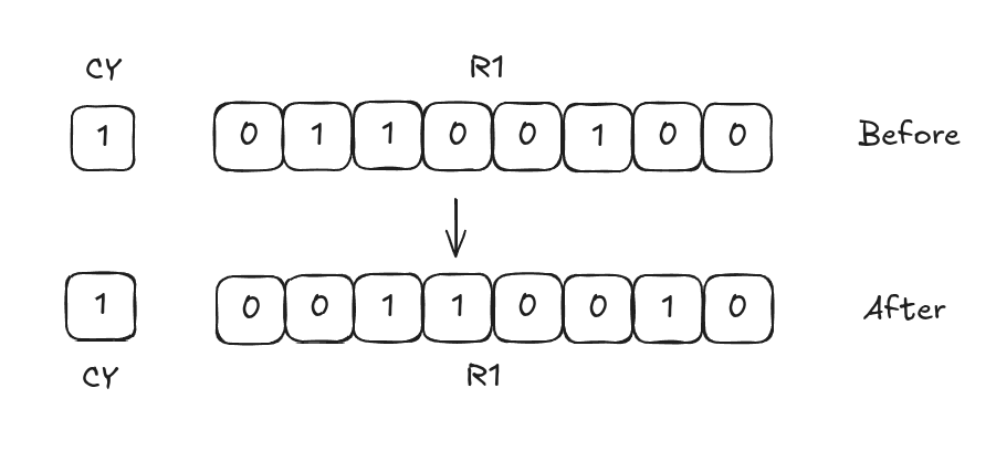
AfterRR R1,
R1=
CY= (Unchanged)
. -
RRC R1
TheRRCinstruction rotates the bits to the right through the Carry Flag. The LSB moves into the Carry Flag, and the previous value of the Carry Flag moves into the MSB.
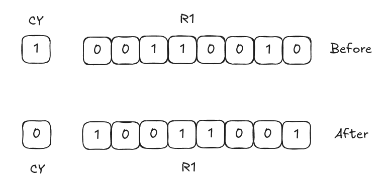 After
After RRC R1,
R1=
CY=
. -
INC R1
TheINCinstruction adds 1 to the current value of the register.
R1=
CY=
. -
SWAP R1TheSWAPinstruction swaps the lower with higher .R1=
CY= (Doesn’t effect carry flag)
. -
RLC R1
TheRLCinstruction rotates the bits to the left through the Carry Flag. The MSB moves into the Carry Flag, and the previous value of the Carry Flag moves into the LSB.
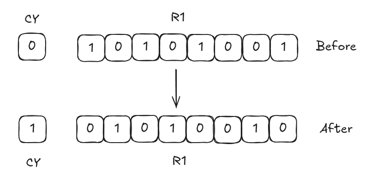 After
After RLC R1,
R1=
CY=
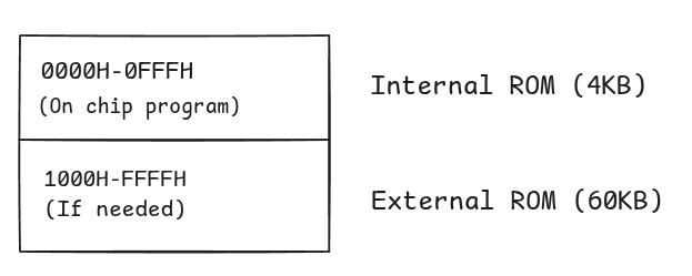
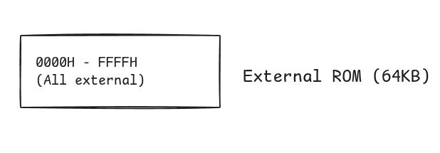
b. Show that the maximum external ROM size of 8051 microcontroller is and in different cases.08
Ans: The 8051 microcontroller architecture supports external memory expansion through a 16-bit address bus, allowing it to address external program memory (ROM) and external data memory (RAM). The maximum addressable external ROM size varies depending on the hardware configuration and the status of the External Access (EA) pin.
- Maximum External ROM = 64KB
This maximum is achieved when the internal ROM is bypassed entirely. When the External Access (EA) pin is connected to ground (), the microcontroller ignores its internal memory and fetches all instructions from the external ROM starting at address . A 16-bit address bus allows the processor to access unique memory locations.
Address bus width = 16 bits
Maximum addressable locations = 2^16 = 65,536 locations
Each location = 1 byte
Maximum external ROM = 65,536 bytes = 64KB
- Maximum External ROM = 60KB
This constraint applies when the microcontroller utilizes its on-chip program memory alongside external expansion. Standard 8051 variants contain of internal ROM located at addresses to . When the External Access (EA) pin is held high (), the processor executes instructions from the internal ROM first. The microcontroller only switches to the external bus for addresses and above, effectively leaving of accessible external program space ().
Total addressable code space = 64KB
Internal ROM space (EA=1) = 4KB
Available external ROM = 64KB - 4KB = 60KB
With (Internal ROM enabled):
 With (External ROM only):
c. Distinguish between Microprocessor and Microcontroller. 02
Ans:
| Microprocessor | Microcontroller |
|---|---|
| CPU is stand-alone. RAM, ROM, I/O are separate. | CPU, RAM, ROM, I/O are on a single chip. |
| Generally large in size. | Small and compact |
| More expensive | Cheaper than Microprocessor |
| Higher power consumption | Lower power consumption |
Question 5
a. Demonstrate how memory is interfaced in 8051 micrcontroller with diagram.10
Question 6
a. With proper diagrams, explain the special function registers (SFR) of a 8051 microcontroller.10
Ans: Special Function Register (SFR) sits on top of 128 byte RAM of 8051 starting from memory location to . Total size of SRF is also 128 bytes.
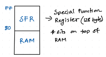
SFR contains registers like microprocessor.
- Accumulator (A & B)
Performs math and logical operations. Mainly works A, involves B for multiplication and division.
| Register | Size | Location |
|---|---|---|
| A | 8 bit | |
| B | 8 bit |
- Status Register (Flag)
Size = 8 Bit Address =
| CY | AX | FO | RS1 | RS0 | OV | - | P |
|---|---|---|---|---|---|---|---|
| Carry | Auxilary | Ext. Ram | Bank | Bank | Overflow | Parity |
| RS1 | RS0 | Bank |
|---|---|---|
| 0 | 0 | |
| 0 | 1 | |
| 1 | 0 | |
| 1 | 1 |
- Pointer Register
To indicate CPU which Bank we are using.
Higher Bank ()
Lower Bank () - Stack Pointer
Address = - I/O Port Register
8 Bit Each
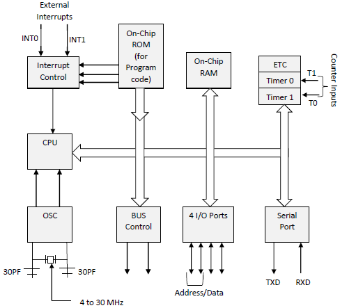
b. Draw the block diagram of a 8051 Microcontroller.08
c. Distinguish between RAM and ROM of 8051 microcontroller. 02
| ROM | RAM |
|---|---|
| Read only memory | Random access memory |
| Program memory | Data memory |
| 4KB ROM | 128 Byte RAM |
| pin works under ROM | Not functional in RAM |
| Non Volatile | Volatile |