The memory banks of a microcontroller is given below. What will be the final values of the registers A & R1, after the execution of the codes?
MOV A, #07H
MOV 04H, 08H
MOV R1, #03H
ADDC A, R1
SWAP R1
CLR C
ORL A, 0AH
XCH A, 0EH
SETB C
ADD A, R1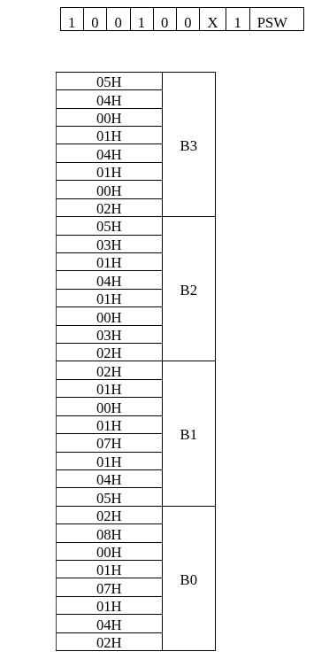
Solution: State of Flag register (i.e. PSW),
| CY | AC | FO | RS1 | RS0 | OV | - | P |
|---|---|---|---|---|---|---|---|
| 1 | 0 | 0 | 1 | 0 | 0 | X | 1 |
Thus, current value of
- Carry Flag = 1 [CY]
- Memory Bank = [RS1 AND RS0]
Note
Memory bank is selected using RS1 and RS0 bit. For details, see Question 6.a from MMAL Final Solve.
Memory addresses of:
We need those addresses during the execution of code.
MOV A, #07HLoad in registerA.
A=MOV 04H, 08HCopy the value of memory bank address08Hto address04H. Currently08Hholds value , which will be copied into address04H.MOV R1, #03HLoad inR1register of current selected bank . The address ofR1is10H.
R1=ADDC A, R1AddAwithR1and carryCY.
A=A+R1+CY
A=
A=SWAP R1Swap the lower nibble with higher nibble ofR1. The value ofR1becomes from .
R1=CLR CClear the value of carry bit.
CY=ORL A, 0AHLogical OR between registerAand memory bank address0AH. CurrentlyA= and0AH= .
A=
A=XCH A, 0EHExchange the value between registerAand memory bank address0EH. CurrentlyA= and0EH= .
A=
0EH=SETB CSet bit of carry flag.
CY=ADD A, R1AddAwithR1.
A=
A=
Thus the final values, A = , R1 =